Flexible, Reconfigurable and Power Adaptive Power Amplifiers for Wireless Communication (ICT R&D Funded)
A frequency agile, power adaptive broadband power amplifier has applications in many fields including high speed mobile data services, defense, jamming devices etc. Also, the RF front end is a major bottle neck in the realization of Software Defined Radio (SDR). This project focuses on the power amplifier design of a reconfigurable frontend required for SDR. The designed amplifier will be useful for Wi-Fi and WiMAX transceivers as well as S-band communication standards. At present, multiband radio transceivers have separate power amplifiers for each band. A single amplifier for multiband operation means smaller size, less power consumption, reduced bill of material and, thus, will be attractive for both civil and military applications in the domestic and international high-tech industries such as Ericsson, Infineon and Huawei.
High Efficiency Power Amplifiers for RF Applications
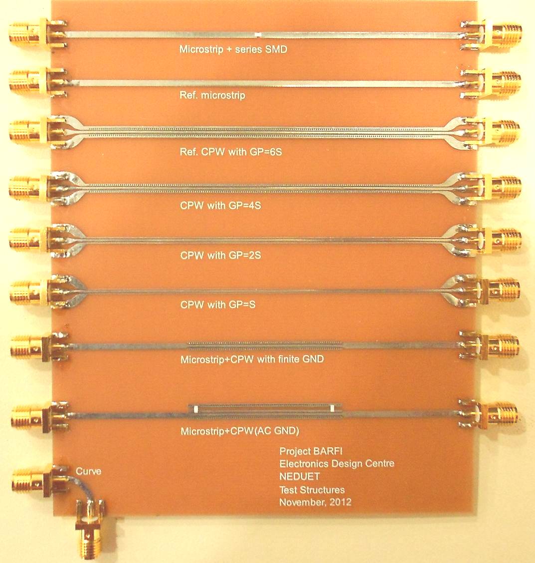
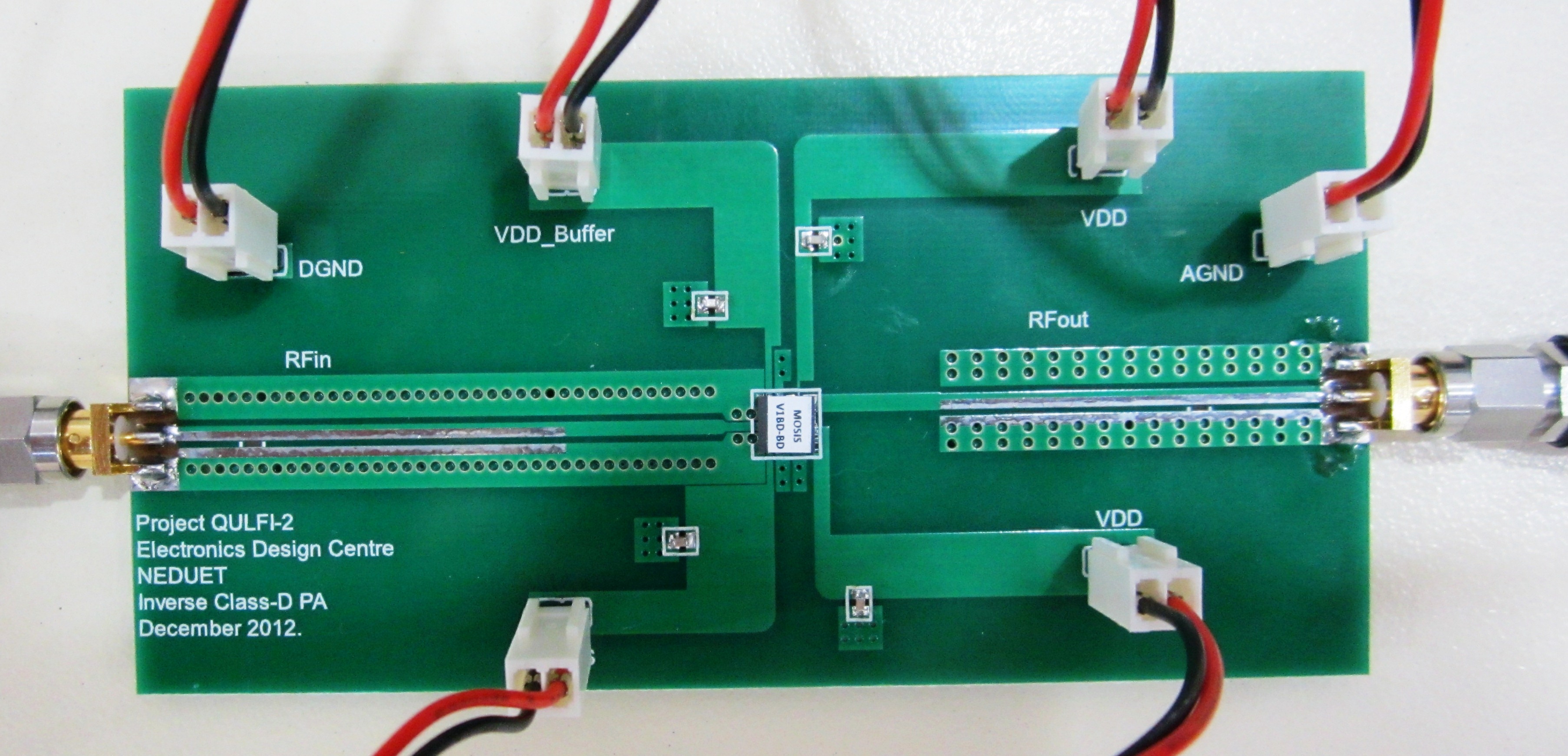
This project involves designing of frequency selective and power adaptive wideband amplifiers. The frequency within a certain band is selected by means of proper termination at the frequency band. A number of power amplifiers are being designed and simulated in Cadence EDA tools. After successful simulation results one design has already been fabricated while second design has been taped out to MOSIS for implementation in IBM 0.13µm CMOS Technology. Extensive collaboration with local industry partner (NESCOM) and academia abroad (Linkoping University, Sweden and METU, Turkey) is being done to benefit from each other's experience and results.