The Device Characterization (DC) lab is a multi-purpose laboratory for on-wafer semiconductor device characterization and integrated circuit testing. The laboratory is equipped with advanced equipment for characterizing electronic devices, power devices, and integrated circuits.
Equipments:
This lab is equipped with following instruments
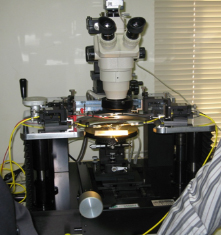
Probe Station (EverBeing PE-4RF)
It has the following specifications:
• Stereo-microscope: 14~90X (~ 220X )
• Gold Plated Vacuum Chuck: 4" / 10µm flatness
• Sample Size: 5x5mm ~ 4"
• Chuck X-Y Stage (10µm resolution)
• Chuck Up/Down (10mm).
It also includes Motic Live Imaging Module. It provides powerful video adjustment, live image transmission and image capturing functions, enabling to view and adjust the real-time image and directly transfer to the main software for further processing or analysis
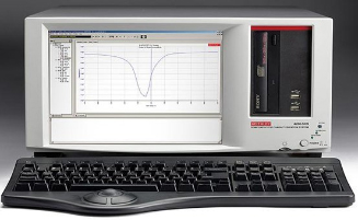
It performs lab grade DC and pulse device characterization, real-time plotting, and analysis with high precision and sub-femto amp resolution. It includes a complete embedded PC with Windows operating system and mass storage. Doping profile extractions, High and low k dielectric characterization, Flash memory testing, Pulse testing of III-V devices, Organic LED characterization, Hall Effect and Van der Pauw testing, High power MOSFET/BJT characterization, Interface charge trap characterization and Solar cell/photovoltaic device characterization can be performed using it.
Keithley 4200-SCS
General measurement by postgraduates and faculty is conducted on equipment dedicated to research in the DC Lab. Students can get hands-on experience in basic device characterization and on-wafer measurement techniques.